L2 BRIDGES
It turns out that L2 cache size changes by manipulating the L2 bridges.

| TEST of the L2 Bridges |
| - | ID 3 | ID 2 | ID 1 | ID 0 | OPN |
| Default ( 256k ) | C | C | C | C | AHM0900AVS3B |
| 128K | C | : | C | C | Tested |
| 64K * | : | C | C | C | DHM0800AVS1BM |
: = L2 Open : Pullup to Vcc_CORE with internal pullup circuit.
C = L2 Closed: Pulldown to Vss with pulldown register.
* It was confirmed by the AMD Athlon DHM 0800AVS1BM.
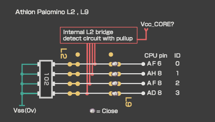
L2, L9 BRIDGES
L2 is connected to AF6, AH8, AF8, and AD8 of CPUpin through L9.
L9 is usually open. Therefore, these pins become active by closing all L9.
However, the function of these pins is not written to Data seet of AMD.
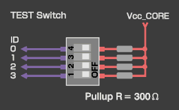
TEST of the ID pins [ AF6, AH8, AF8, AD8 ]
As follows, I connected the switch to these pins
.....see Pin Descriptions
| TEST of the ID pins |
| - | ID 3 | ID 2 | ID 1 | ID 0 |
| L2 Cache size | AD8 | AF8 | AH8 | AF6 |
256K
WCPUID | L | L | L | L |
| L | L | L | H |
| L | L | H | L |
| L | L | H | H |
128K
WCPUID | L | H | L | L |
| L | H | L | H |
| L | H | H | L |
| L | H | H | H |
64K
WCPUID | H | L | L | L |
| H | L | L | H |
| H | L | H | L |
| H | L | H | H |
| H | H | L | L |
| H | H | L | H |
| H | H | H | L |
| H | H | H | H |
H = SW-ON : Pullup to Vcc_CORE with 300(ohms).
L = SW-OFF : Default LO with internal pulldown register.
Probably I think that it is as follows.
| Configuration of the ID pins |
| - | ID 3 | ID 2 | ID 1 | ID 0 |
| L2 Cache size | AD8 | AF8 | AH8 | AF6 |
Default
( 256k ) | L | L | L | L |
| 128K | L | H | - | - |
| 64K | H | - | - | - |
H= SW-ON: Pullup to Vcc_CORE with 300(ohms).
L= SW-OFF: Default LO with internal pulldown register.
- = Don't care? or an unknown factor.....
Data
The voltage measurement result of the ID pins[ AF6, AH8, AF8, AD8 ]
with external pullup register

System configuration
CPU : Mobile Athlon4-900
OPN : AHM 0900AVS3B
Clock : 1.1GHz
Vcc_CORE : 1.6V
Mother : MSI K7TPro2A
OS : Windows 98
Special thanks and Reference
- JOHN CARCICH'S HOME PAGE
- Page 0 Final Decoding Palomino Bridges.
Soft ware
- H.Oda!'s HomePage : WCPUID
- http://www.h-oda.com/
|

|