Athlon XP [ Paromino & Morgan ]
The following report is applicable the Barton and Thoroughbred.
However, my presumed part is contained. Please confirm for yourself.
Multiplier Signal Circuits
We think that the multiplier of Palomino is as follows.
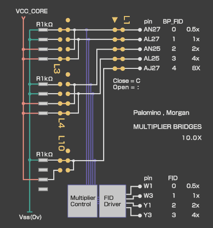
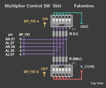
Multiplier control circuit for the palomino
If you are using Motherboard which cannot control the Multiplier, the following circuits are added to it.
The multiplier is controllable by this circuit.
It is not necessary to touch the FIDpins.
BP_FID[4:0] SYSCLK Multiplier Combinations
| Multiplier | Clock
(FSB133) | BP-FID[4:0] | Model# |
| 5.0x | 667M | CC:CC | - |
| 5.5x | 733M | CC:C: | - |
| 6.0x | 800M | CC::C | - |
| 6.5x | 867M | CC::: | - |
| 7.0x | 933M | C:CCC | - |
| 7.5x | 1.00G | C:CC: | - |
| 8.0x | 1.07G | C:C:C | - |
| 8.5x | 1.13G | C:C:: | - |
| 9.0x | 1.20G | C::CC | - |
| 9.5x | 1.27G | C::C: | - |
| 10.0x | 1.33G | C:::C | 1500+ |
| 10.5x | 1.40G | C:::: | 1600+ |
| 11.0x | 1.47G | CCCCC | 1700+ |
| 11.5x | 1.53G | CCCC: | 1800+ |
| 12.0x | 1.60G | CCC:C | 1900+ |
| 12.5x | 1.67G | CCC:: | 2000+ |
| Multiplier | Clock
(FSB133) | BP-FID[4:0] | Model# |
| 13.0x | 1.73G | :C:CC | 2100+ |
| 13.5x | 1.80G | :C:C: | - |
| 14.0x | 1.87G | :C::C | - |
| *** | - | :C::: | - |
| 15.0x | 2.00G | ::CCC | - |
| *** | - | ::CC: | - |
| 16.0x | 2.13G | ::C:C | - |
| 16.5x | 2.20G | ::C:: | - |
| 17.0x | 2.27G | :::CC | - |
| 18.0x | 2.40G | :::C: | - |
| *** | - | ::::C | - |
| *** | - | ::::: | - |
| 3.0x | - | :CCCC | - |
| *** | - | :CCC: | - |
| 4.0x | - | :CC:C | - |
| *** | - | :CC:: | - |
: = down (logic level of 1) , C = Up (logic level of 0)
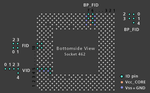
Pin diagram of Socket A
Copyright 2002 ita. All rights reserved. Never reproduce or republicate without written permission.
|

|